 1 Introduction When a DC voltage acts on an insulator, the resulting current is composed of a charging current, an absorption current, and a leakage current. The charging current and the absorption current decrease from time to time, and only the leakage current and No time.
 The insulation resistance test is to measure the leakage current value of the electrical equipment through the meter. Usually the meter displays this current value as the insulation resistance value (MΩ). In order to reduce the influence of the initial charge current, the insulation resistance value after 1 min of pressurization is generally taken as the measurement value R60; if the value R15 of 15 s is read at the same time, the absorption ratio K=R60/R15 can be calculated. The comparisons reflect the local defects of large-scale power transformers are more sensitive, such as the transformer oil containing moisture, local weaknesses or dirt in the casing and coils.
Insulation resistance and absorption ratio are all sensitive indicators to judge whether the insulator is damp.
Insulation resistance test instrument used is mainly megohmmeter, commonly known as shaking table. Traditional megohmmeters have 500V, 1000V, and 2500V DC voltages emitted from hand-cranked generators. The measurement range of insulation resistance varies depending on the megohmmeter type. Different types or voltage grades should be selected according to requirements. Megohmmeter. When using the hand-type megohmmeter, the user should also keep the hand cranking speed at the rated rotation speed of 120r/min. Therefore, it is inconvenient to use it.
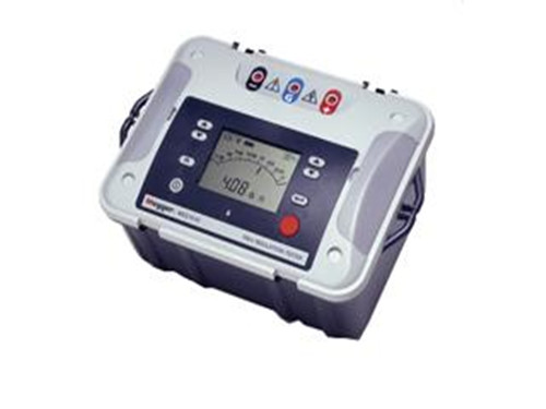
The portable insulation resistance tester mentioned in this article is powered by a 12V battery. The single-ended flyback switching power supply can generate stable 500V, 1000V, 1500V, 2000V and 2500V series voltages. The SCM system also performs measurement sampling, data processing and display. control. With a small size, light weight, fast response and so on. The following mainly introduces the circuit principle and manufacturing method of its power supply.
2 The composition and working principle of the power circuit Figure 1 shows the circuit principle of the high voltage DC power supply for the digital insulation resistance tester. The power supply is a 12V battery, and it is still required to ensure the normal operation of the system when the voltage is above 10V. The switching device uses the TWH8751 type switch integrated circuit. For the characteristics of small circuit output power, high output voltage, and small size, a single-ended flyback converter topology is used. The secondary windings of high-frequency switching transformers have five groups corresponding to 500V, 1000V, 1500V, 2000V and 2500V DC. The tap can be selected by the user according to the needs of the multi-shot knob switch gear to switch the secondary winding tap and the corresponding output voltage sampling resistor at the same time. According to the sampling of the output voltage and current, the control circuit will change the conduction width of the switching device in time so as to stably output the desired voltage and provide over-voltage over-current protection.
2.1 TWH8751 switch integrated circuit TWH8751 power switch integrated circuit adopts TOP-220 package form, the inner circuit is composed of input stage, buffer amplifier and Darlington power output stage, and has feedback loop and current reduction type output protection circuit. Strong. There are 5 pin out pins, as shown in the corresponding part of the figure in Figure 1. The pin functions are: input (IN), strobe (ST), ground (GND), output (OUT), and power supply. End (VCC). When the pin 2 strobe terminal level is ≥1.6V, the pin 1 input has no control over the output pin (pin 4), that is, the final Darlington transistor is turned off and the circuit has no output; only pin 2 is low (< In 1.2V), the signal applied to pin 1 can effectively control the level of the pin 4 output.
The TWH8751's input and strobe inputs have very low input control currents of only 100 to 200μA, while the maximum allowable current at the output is 2A. There is also a current-reducing protection circuit. When the output current exceeds 3A, the protection circuit can automatically reduce the output current to about 1A. After the output is turned off, the integrated switching circuit will return to the 2A output load capacity.
In this example, pin 2 is grounded so that the output of pin 4 is directly controlled by pin 1 . The resistor R6 between the pin 5 and the power supply acts as a current limiter and must be used, about 50Ω. The switching control signal of TL494 also passed the current-limiting resistor R7, which can reduce the operating power of the chip to facilitate the heat dissipation.
Since the power of the system itself is small, the switching device is only required to withstand twice the reverse voltage of the power supply voltage. Therefore, the selection range of the switch tube is very large, and MOS transistors or IGBTs can also be selected because of their presence between the gate and the drain. Larger junction capacitances have a greater impact on the switching speed, and also require a higher driving voltage, and electrostatic protection between the gate and drain must be considered. The experimental comparison also shows that the TWH8751 has good switching characteristics and wide input voltage adaptation range under this system condition, and the circuit is also very simple. Therefore, it is appropriate to use the TWH8751 switch IC.
2.2 Pulse width modulation control circuit part TL494 is a mature constant frequency pulse width modulation integrated circuit, the internal structure of the chip and its specific function are not repeated. A brief description of the corresponding parts of the system will be given with reference to FIG.
The system pulse frequency can be approximated by C1 and R1 according to equation (1). A reasonable combination of timing resistors and capacitor values ​​can increase the accuracy of the reference voltage and the system's ability to carry loads. In this example, C1 takes 0.01μF, and fosc is adjusted to about 30kHz. The output terminal of the chip pin 13 is grounded so that the two output transistors inside the chip output in a synchronous manner to ensure the output current. If the switching transistor uses IGBT, the driving signal is directly driven without amplification; the dead-zone control voltage of pin 4 is used to limit the maximum on-time of the switching device. When ton=T/2, the maximum voltage of the switching terminal is 2 times the power supply voltage, when the conduction time increases, you need to use a higher pressure switch.
R19 in Figure 1 is a small precision resistor used to sample the load current and forms a comparator with one of the TL494 on-chip error amplifiers for output over-current protection. R9, R10 and C4 form an analog PI regulator for stable regulation of negative feedback of the output voltage. R11 is the balance resistance of the PI regulator. The expected feedback voltage on R13 ~ R17 should be 5V, according to which you can calculate the resistance of R13 ~ R17, for example, in the selected switch mode marked in Figure 1, it should meet R14 / (R14 + R18) = 5V/1000V (2)
Among them, R18 should be chosen large enough to reduce its shunt to the load, thereby improving the efficiency of the entire system.
The voltage regulator D2 in the circuit is used for overvoltage protection of the control part to prevent the high voltage from being switched in when the switch is switched.
2.3 Inverter Some converters use single-ended flyback because the topology can be easily stepped up or stepped down, which is particularly suitable for low power applications. In FIG. 1, when the switch is turned on, the battery voltage is applied to the primary winding of the transformer T1, so that a positive and negative negative voltage is induced on the secondary winding. The rectifier diode D1 is in an off state, and the power can only be The form of magnetic energy is stored in the transformer; when the switch is turned off, the voltage of the secondary winding becomes positive and negative, and the rectifier diode D1 is turned on, and the magnetic field energy storage is released to the load through the diode. Throughout the working process, the transformer acts both as a booster and as an energy storage inductor.
The circuit parameters should ensure that the circuit works in the continuous mode of magnetizing current, that is, the secondary current is still greater than zero at the end of switch off time toff. In theory, this means that it is necessary to relatively increase the primary inductance L1 of the transformer or increase the on-time of the switch tube. Ton to help increase energy storage. On the other hand, in order to ensure that the magnetic flux of the transformer is reset and the magnetic saturation of the iron core is prevented from causing damage to the switch tube, it is necessary to leave a margin for the cutoff time of the switch tube. The actual system needs multiple considerations. The optimum matching of various parameters can be used to make a qualitative reference using equation (3). As long as the system is satisfied, the magnetizing current is continuous and the output voltage has nothing to do with the load. As long as it is satisfied then the volt-second balance condition is satisfied and the magnetic flux can be reset.
Where: N1 is the primary winding number of the transformer;
N2 is the secondary winding number of the transformer;
L1 is the equivalent inductance of the primary winding of the transformer;
RL is the resistance of the output equivalent load;
Vo is the output DC voltage;
Vi is the transformer input voltage, the battery voltage.
The calculation of the inductance L1 of the primary winding of the transformer should be designed according to the minimum value of the output voltage, that is, 500V, because the corresponding inductance is maximum at this time. After determining the number of turns of the primary winding, the secondary corresponding values ​​are calculated according to equation (4). Number of winding turns.
According to the experiment, the primary power supply N1 is 4 turns, and the secondary is a tapper every 200 turns, totaling N2 is 1000 turns. The ferrite core selects the PQ2020 type, and the core material is equivalent to the Japanese H7C4 core material.
3 Process Structure Design High-voltage power supply for the treatment of high-voltage parts, the wiring of the low-potential part, the selection and layout of circuit components, the layout of the control board must have appropriate insulation considerations, at the same time switching power supply specific noise issues, etc. The structural design of high-voltage power systems has become a very difficult problem and requires a certain amount of production experience.
The core components of the circuit are high-voltage transformers because of their high voltage, many turns, thin conductors, narrow spacing between adjacent conductors, and large parasitic capacitances between lines and between layers, allowing the energy to be charged and discharged through this capacitor during each cycle. Large, but these energy is not completely consumed in the secondary side, but in the primary switch has produced a lot of loss, and produce a loud noise. Therefore, the primary winding should use honeycomb or segmented winding methods to reduce parasitic capacitance. And it is better to wrap the primary winding around the secondary outer layer to reduce leakage inductance and facilitate debugging.
In order to prevent high-voltage ignition, components around the high voltage should not have sharp corners, and should maintain a proper space distance, the transformer core uses a ferrite core with a cylindrical core, allowing a small space in the conditions, Also, the thickness of the interlayer insulation paper should be increased as much as possible, and the tapped portion is led through the insulating sleeve. After the transformer is made, it should be immersed in paint several times and encapsulated with silicone rubber to improve the insulation performance.
At the same time, the wiring in the loops of components (switches, transformers, and fast recovery diodes D1) subjected to high di/dt, dv/dt should be as short as possible to reduce the effective area and circuit losses of the electromagnetic interference source.
76.png)

1.Novel appearance and bright appearance
2.The hot air distribution is uniform, and the drying efficiency is increased
3.All digital P.I.D control
4.Cylinder and internal parts are made of stainless steel
5.The charging barrel is separated from the bottom, the material cleaning is convenient, and the material changing is quick
6.Overheat protection device, can reduce the accident caused by man-made or mechanical failure
Adhering to the " integrity,innovation,mutual win,beyond" business concept, and shoulder "do the best plastic&rubber auxiliary machine in China" corporate mission, according the market and customer demand-driven,scientific management,fiexible production. For the customer,supplier,employees,enterprise,society to create greater value, is committed to be the most influential plastic&rubber machine industry leader.
Plastic Hopper Dryer,Hopper Type Plastic Dryer,Hot Wind Style Plastic Hopper Dryer,Hopper Dryer For Plastic
Ningbo Tongyong Plastic Machinery Manufacturering Co. Ltd. , https://www.tongyong-machinery.com