[China Instrument Network Instrument Development] Electronic Conductive Metal-Organic Frameworks (EC-MOFs) materials are a new class of conductive materials formed by metal ion or metal ion clusters and organic ligands that self-assemble through coordination bonds. Porous crystalline materials are a new class of crystalline materials that combine porosity, selectivity, and semiconductor properties. Due to its abundant designable crystal structure and adjustable electron energy band structure, EC-MOFs materials are used as active functional components in novel field effect transistors, lithium batteries, supercapacitors, gas sensors, and other semiconductor devices. Has high research value and application potential.
However, most of the applications of reported EC-MOFs materials have been in the form of powders or thick films, and the large particle size and grain boundaries have limited the electronic and material transport in electrical devices. It is well known that the quality of thin films is one of the important determinants of high performance devices. The layer-by-layer (LbL) liquid phase epitaxy method is an effective method for preparing a uniform thickness and homogeneous MOFs film. However, only some MOFs with special secondary building units (SBUs) can use the LbL method to prepare thin films. The application of the LbL method to the controlled epitaxial growth of EC-MOFs conductive films has not been reported so far.
Under the support of the National Natural Science Foundation of China, the Scientific Research Equipment Development Project of the Chinese Academy of Sciences and the leading scientific projects of the Chinese Academy of Sciences, the research team headed by Xu Gang, a researcher at the State Key Laboratory of Structural Chemistry of the Fujian Institute of Materials Structure, Chinese Academy of Sciences, is thin and controllable, and Progress has been made in the research of durable EC-MOFs films and devices.
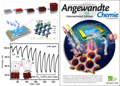
Yao Mingshui, a research fellow with the research group, and Lu Xiaojing, a master student, used the LbL spray method to prepare for the first time an EC-MOFs film with thickness and quality controllable on a nanometer scale. EC-MOFs thin film growth is based on a class of chemically stable hexagonal EC-MOFs material Cu3(HHTP)2 (HHTP=2,3,6,7,10,11-hexahydroxytriphenylene), which is in ab Cu-HHTP two-dimensional conductive structure was formed in the direction, and a honeycomb-like microporous structure was stacked in the c-axis direction in a slightly slip ABAB mode. The room temperature electrical conductivity of the film reached 2 S·m−1. The Cu3 (HHTP) 2 film prepared by this method not only has a single layer thickness controllable ~2 nm, a surface roughness <5 nm, but also has a good crystal orientation perpendicular to the substrate direction along the [001] direction. These advantages give it great potential for application in high-efficiency electrical devices. As an example of application, Cu3(HHTP)2 films grown on prefabricated sapphire substrates are applied directly to room-temperature chemiresistor gas sensors. The experimental results show that at room temperature, the thinner the film, the better the gas diffusion and charge transport ability, and the stronger the gas detection capability. Among them, the thickness of 20nm thick Cu3(HHTP)2 film is the best, and the room temperature resistance of 100ppm can be up to 129%, and the ammonia gas shows good selectivity and long-term stability (remaining ~90% response value after 96 days). The analysis shows that the p-type response is due to the increase in Fermi level (n-type doping effect) due to the reductive ammonia adsorption, the carrier concentration decreases, resulting in a drop in current; high selectivity is mainly due to ammonia and Cu sites. Strong interaction with ligands. At the same time, the response of the Cu3(HHTP)2 thick film sensor has been improved by more than an order of magnitude because of the smooth surface of the film, and the close and oriented packing of particles, further enhancing the charge transport and mass transfer capability.
The relevant results were published in "German Applied Chemistry" and were selected as the cover of the current period. Research work has received attention and coverage from academic platforms such as Kongdao, Nanoman, and Research.
(Original Title: Research Progress on Conductive MOF Thin Film Devices Made by Fujian Construction)
Kids role play house&games (My town Playground) is new play equipment. Role play is an irreplaceable part on child develpment help kids ge into character and imitate the normal life of adult and fictional performances, help them creativity comunication, build confidence, problem sloving both physical and spiritual. Aware of real life, learn and make friends by role play.
Kids Indoor Role Play,Indoor Role Playing,Children Indoor Role Play,Kids Role Play
HANGZHOU JOY TECHNOLOGY CO., LTD. , https://www.joyplaypark.com