1. Crystals and crystals In general, we call crystals and Oscillators both crystals. This is not an appropriate name.
The passive crystal is a non-polar element with two pins, as shown in Figure 1(a). In normal operation, an external circuit is required to generate an oscillating signal, which does not require a separate external power supply.

The active crystal oscillator generally has four pins, as shown in Figure 1 (b), which integrates components such as quartz crystals, transistors, and resistors and capacitors. The crystal oscillator is a complete oscillator, and it only needs to work properly with an appropriate power supply. No additional external circuitry is required.
2. Cost Analysis When designing, the engineer should reduce the design cost as much as possible. From Table 1 it can be seen that the crystal-to-crystal oscillator circuit can reduce the cost of the crystal by 60%.
3. The crystal oscillator is composed of a crystal plus an unbuffered inverter and other components to form a crystal oscillator circuit. The principle and components are shown in Figure 2.

The choice of resistance and capacitance in the circuit depends on the gain of the inverter, frequency stability, power consumption, crystal characteristics, and startup time. The recommended parameters are shown in Table 2.
The passive crystal is a non-polar element with two pins, as shown in Figure 1(a). In normal operation, an external circuit is required to generate an oscillating signal, which does not require a separate external power supply.
Figure 1 Crystal and Crystal
The active crystal oscillator generally has four pins, as shown in Figure 1 (b), which integrates components such as quartz crystals, transistors, and resistors and capacitors. The crystal oscillator is a complete oscillator, and it only needs to work properly with an appropriate power supply. No additional external circuitry is required.
2. Cost Analysis When designing, the engineer should reduce the design cost as much as possible. From Table 1 it can be seen that the crystal-to-crystal oscillator circuit can reduce the cost of the crystal by 60%.
Table 1 price comparison
Crystal oscillator circuit
element
price
Crystal price
Active Crystal Circuit
Active Crystal
About 4 yuan
About 4 yuan
Passive crystal to active crystal
Circuits
Passive crystal
0. 8 yuan
About 2.3 yuan
Unbuffered inverter
0. 5 yuan
Resistor-capacitor
0.1 yuan or less
3. The crystal oscillator is composed of a crystal plus an unbuffered inverter and other components to form a crystal oscillator circuit. The principle and components are shown in Figure 2.
Figure 2 Crystal oscillator circuit composed of an unbuffered inverter and a crystal
The choice of resistance and capacitance in the circuit depends on the gain of the inverter, frequency stability, power consumption, crystal characteristics, and startup time. The recommended parameters are shown in Table 2.
Table 2 parameter selection

Labeling
name
Preferences
R F
Feedback resistance
1~10MΩ
U1
Unbuffered inverter
Reference selection: NXP-74HC2GU04; Â Â ON-NL27WZU04 ; TI- SN74LVC2GU04 ;
X1
Crystalline
The load capacitance CL of the crystal is related to the parameter selection of R S , C1 , C2
R S
Isolation resistance
About equal to the capacitance of C2
C1
capacitance
C2
capacitance
U1: Increase U1B mainly to increase output capacity. The type of unbuffered inverter can be selected from NXP, ON, TI and other manufacturers of double inverter chip.
RF: The feedback resistor of the inverter, which biases the inverter in the linear region. The RF value chosen needs to be large enough so that the input impedance of the inverter can match the crystal. Normally, the value chosen is between 1MΩ and 10MΩ.
RS: Separates the output of the inverter from the crystal to prevent spurious high-frequency oscillations in order to obtain a good waveform. Acceptable results can be obtained by choosing a value that is approximately equal to the capacitive reactance (RS≈XC2).
C1, C2: When selecting the values ​​of C1 and C2, make the parallel value of C1 and C2 equal to the recommended load capacitance (CL) specified in the crystal data table. In addition, the choice of capacitance is also related to the crystal's start-up time, phase shift, resonant frequency, and so on.
4. Parametric test When testing the circuit, we used three different frequency crystals (see Table 3) and three manufacturers of unbuffered inverters for combinatorial testing. The test results are shown in Table 4.
Table 3 Crystal parameters
Nominal frequency
Load capacitance
Adjustment frequency difference
Operating temperature
Temperature difference
16.00MHz
20pF
±30 ppm
-20 °C ~+70 °C
±30 ppm
24.00MHz
20pF
±30 ppm
-20 °C ~+70 °C
±30 ppm
27.12MHz
20pF
±30 ppm
-20°C ~+70 °C
±30 ppm
Table 4 Test Statistics of Various Circuits
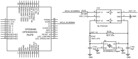
When customers M3352_YP do peripheral circuits, if you need to use Fast Ethernet function, you need to add PHY circuit. PHY chip can usually choose DSZ8041 or DP83848. When using RMII interface, no matter what type of PHY chip is selected, it needs to be PHY. The chip provides a 50MHz CLK signal. In order to reduce the cost, 50.000M crystal clock + NL27WZU04 can be used to provide 50.000M clock source for the PHY.
Model and Manufacturer
Nominal frequency
Frequency range (MHz)
Test frequency (MHz)
Duty cycle
Oscillation time
NL27WZU04(ON)
24.00MHz
23.999280~24.000720
23.999529~23.999535
52.16%
27us
NL27WZU04(ON)
27.12MHz
27.119186~27.120814
27.120630~270120635
52.30%
44us
74HC2G104 (NXP)
16.00MHz
15.999520~16.000480
16.000111~16.000114
51.12%
150us
74HC2G104 (NXP)
24.00MHz
23.999280~24.000720
23.998941~23.998946
50.60%
140us
SN74LVC1GX04(TI)
16.00MHz
15.999520~16.000480
16.000033~16.000036
51.76%
130us
SN74LVC1GX04(TI)
27.12MHz
27.119186~27.120814
27.120341~27.120345
52.85%
37.5us
Remarks:
Test tool: Tektronix oscilloscope; multifunction counter - SP1500B ;
Test temperature: 25 °C ±2 °C. ;
Test voltage: 3.3V .
Frequency: It can be known from the adjustment frequency difference (25°C±2°C) of the crystal that the crystal frequency is allowed to vary within its tolerable frequency range. The test frequency in Table 4 is within the allowable range and the range of variation is small.
Duty cycle: The digital system does not require strict duty cycle. If used in precise duty cycle, the user needs to filter and test the parameter.
Start-up time: Use the oscilloscope's level trigger function to measure the time from system power-up to stable waveform output.
High and low temperature test: according to the working temperature of the crystal, the output frequency, duty cycle and other parameters of the circuit at 85°C, 70°C, 50°C, 25°C, 0°C, -20°C, and -40°C were respectively tested and recorded. The crystal oscillator can start smoothly and the parameters are normal. Due to the large number of data and limited space, it will not be listed here.
5. Conclusion The use of passive crystal active crystal oscillator is not only technically feasible, but also can reduce costs.
6. Applications TI launched the low-cost, high-performance Cortex-A8 core AM335x series processor for industrial control in 2011. Zhiyuan Electronics adopted the AM335x processor and introduced the M3352_YP core board in the stamp hole package to meet customer requirements. The need for stability.
Duty cycle: The digital system does not require strict duty cycle. If used in precise duty cycle, the user needs to filter and test the parameter.
Start-up time: Use the oscilloscope's level trigger function to measure the time from system power-up to stable waveform output.
High and low temperature test: according to the working temperature of the crystal, the output frequency, duty cycle and other parameters of the circuit at 85°C, 70°C, 50°C, 25°C, 0°C, -20°C, and -40°C were respectively tested and recorded. The crystal oscillator can start smoothly and the parameters are normal. Due to the large number of data and limited space, it will not be listed here.
5. Conclusion The use of passive crystal active crystal oscillator is not only technically feasible, but also can reduce costs.
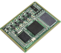
6. Applications TI launched the low-cost, high-performance Cortex-A8 core AM335x series processor for industrial control in 2011. Zhiyuan Electronics adopted the AM335x processor and introduced the M3352_YP core board in the stamp hole package to meet customer requirements. The need for stability.
Figure 3M3352 Stamp Hole Core Board
When customers M3352_YP do peripheral circuits, if you need to use Fast Ethernet function, you need to add PHY circuit. PHY chip can usually choose DSZ8041 or DP83848. When using RMII interface, no matter what type of PHY chip is selected, it needs to be PHY. The chip provides a 50MHz CLK signal. In order to reduce the cost, 50.000M crystal clock + NL27WZU04 can be used to provide 50.000M clock source for the PHY.
Figure 4 passive crystal active crystal oscillator typical application circuit